Recently, Government is seeking applications from startups and MSME for design linked initiatives.
About Design Linked initiatives:
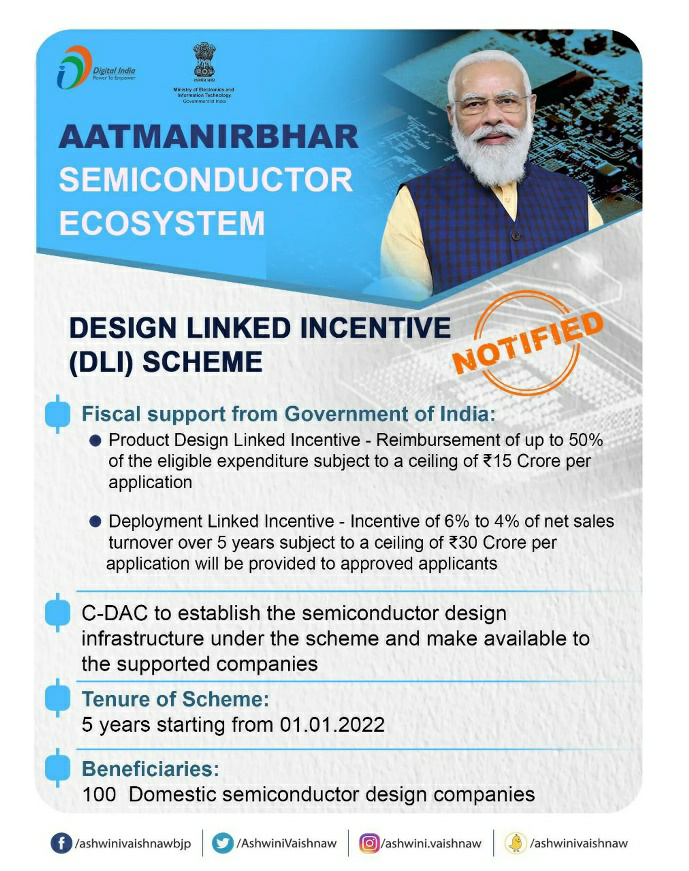
Announced by MeitY in December 2021.
As part of this, financial incentives and design infrastructure support for domestic companies, start-ups and MSMEs at various stages of developing and deploying semiconductor designs for integrated circuits (ICs), chipsets and system-on-chips (SoCs) will be provided.
Systems and IP cores have extended Semiconductor Linked Design for over five years.
Objective:
To create a vibrant semiconductor chip design ecosystem in the country.
Promote domestic manufacturing of semiconductors and related equipment.
The program aims to provide companies in the semiconductor and display manufacturing and design industries with a globally competitive incentive package.
Implementation:
The Center for Development of Advanced Computing (CDAC), a scientific society operated under MeitY, acts as a node agency for the implementation of DLI schemes.
Components:
There are three components Chip design infrastructure support:
As part of this, CDAC has established the India Chip Center to host and provide state-of-the-art design infrastructure (ie, EDA tools, IP cores, MPW (multi-project wafer manufacturing) and post-silicon verification support).
Easier access to supported enterprises.
Incentives related to product design: Under this program, approved applicants involved in semiconductor design are eligible for a refund of up to 50% of eligible expenses, subject to a maximum of 15 chlores per application.
Mission-related incentives:
These include approved applicants whose semiconductor designs for integrated circuits (ICs), chipsets, system-on-chip (SoC), system & IP cores, and semiconductor link designs are used in electronic products.