Description
Disclaimer: Copyright infringement not intended.
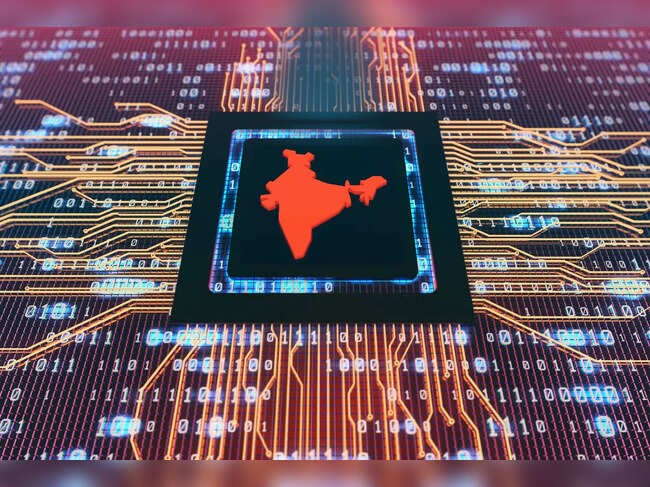
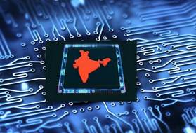
Context
- India Semiconductor Mission (ISM) has been setup as an Independent Business Division within Digital India Corporation.
Details
- ISM has all the administrative and financial powers and is tasked with the responsibility of catalysing the India Semiconductor ecosystem in manufacturing, packaging and design.
- ISM has an advisory board consisting of some of the leading global experts in the field of semiconductors. ISM is serving as the nodal agency for efficient, coherent and smooth implementation of the programme for development of semiconductor and manufacturing ecosystem in India.
.jpg)
Objectives of ISM are as under:
- Formulate a comprehensive long-term strategy for developing sustainable semiconductors and display manufacturing facilities and semiconductor design eco-system in the country in consultation with the Government ministries / departments / agencies, industry, and academia.
- Facilitate the adoption of secure microelectronics and developing trusted semiconductor supply chain, including raw materials, specialty chemicals, gases, and manufacturing equipment.
- Enable a multi-fold growth of Indian semiconductor design industry by providing requisite support in the form of Electronic Design Automation (EDA) tools, foundry services and other suitable mechanisms for early-stage startups.
- Promote and facilitate indigenous Intellectual Property (IP) generation.
- Encourage, enable and incentivize Transfer of Technologies (ToT).
- Establish suitable mechanisms to harness economies of scale in Indian semiconductor and display industry.
- Enable cutting-edge research in semiconductors and display industry including evolutionary and revolutionary technologies through grants, global collaborations and other mechanisms in academia / research institutions, industry, and through establishing Centres of Excellence (CoEs).
- Enable collaborations and partnership programs with national and international agencies, industries and institutions for catalyzing collaborative research, commercialization and skill development.
- ISM has been working as nodal agency for the Schemes approved under Semicon India Programme.
- ISM has also been engaging with various stakeholders of Semiconductors and Display ecosystem to attract the investments in India.
Must Read: https://www.iasgyan.in/daily-current-affairs/semiconductor
.jpg)
- Government is very focused on its important objective of building the overall semiconductor ecosystem and ensure that, it in-turn catalyses India’s rapidly expanding electronics manufacturing and innovation ecosystem.
- Government has approved the Semicon India programme for the development of semiconductor and display manufacturing ecosystem in the country.
Following four schemes have been introduced under the aforesaid programme:
- ‘Modified Scheme for setting up of Semiconductor Fabs in India’ for attracting large investments for setting up semiconductor wafer fabrication facilities in the country to strengthen the electronics manufacturing ecosystem and help establish a trusted value chain. The Scheme extends a fiscal support of 50% of the project cost on pari-passubasis for setting up of Silicon CMOS based Semiconductor Fab in India.
- ‘Modified Scheme for setting up of Display Fabs in India’ for attracting large investments for manufacturing TFT LCD or AMOLED based display panels in the country to strengthen the electronics manufacturing ecosystem. Scheme extends fiscal support of 50% of Project Cost on pari-passubasis for setting up of Display Fabs in India.
- ‘Modified Scheme for setting up of Compound Semiconductors / Silicon Photonics / Sensors Fab / Discrete Semiconductors Fab and Semiconductor Assembly, Testing, Marking and Packaging (ATMP) / OSAT facilities in India’shall extends a fiscal support of 50% of the Capital Expenditure on Pari-passu basis for setting up of Compound Semiconductors / Silicon Photonics (SiPh) / Sensors (including MEMS) Fab/ Discrete Semiconductor Fab and Semiconductor ATMP / OSAT facilities in India.
- ‘Semicon India Future Design: Design Linked Incentive (DLI) Scheme’ offers financial incentives, design infrastructure support across various stages of development and deployment of semiconductor design for Integrated Circuits (ICs), Chipsets, System on Chips (SoCs), Systems & IP Cores and semiconductor linked design. The scheme provides “Product Design Linked Incentive” of up to 50% of the eligible expenditure subject to a ceiling of ₹15 Crore per application and “Deployment Linked Incentive” of 6% to 4% of net sales turnover over 5 years subject to a ceiling of ₹30 Crore per application.
https://pib.gov.in/PressReleaseIframePage.aspx?PRID=1885367